Address
Room 2301C, 23rd Floor, Building 1, jinghu Commercial center, No, 34, Liangzhuang Street, Eri District, Zhengzhou City, Henan province
Work Hours
Monday to Friday: 7AM - 7PM
Weekend: 10AM - 5PM
Address
Room 2301C, 23rd Floor, Building 1, jinghu Commercial center, No, 34, Liangzhuang Street, Eri District, Zhengzhou City, Henan province
Work Hours
Monday to Friday: 7AM - 7PM
Weekend: 10AM - 5PM

In today’s highly information-driven world, chips have become an indispensable infrastructure. From smartphones and personal computers to servers, supercomputers, and even cutting-edge technologies such as artificial intelligence, the Internet of Things, and autonomous driving, all rely on high-performance, highly reliable chips. The performance of chips directly determines the operating speed, power consumption, and level of intelligence of electronic devices.
Chip manufacturing is an extremely complex and precise engineering process, involving multiple disciplines such as materials science, physics, chemistry, and electrical engineering. Its manufacturing process requires hundreds of steps, each placing extremely high demands on the performance of materials and equipment. In recent years, as Moore’s Law approaches its physical limits, chip manufacturing faces increasing challenges. To overcome these bottlenecks, researchers are constantly exploring new materials and processes. Among these, rare earth elements, due to their unique optical, electrical, and magnetic properties, are playing an increasingly important role in chip manufacturing.

Application of rare earth elements in photolithography
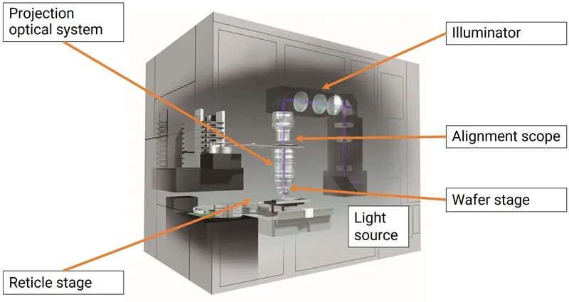
Photolithography is one of the most critical processes in chip manufacturing, and its resolution directly determines the chip’s integration density. Photolithography technology defines various microstructures on the chip by transferring designed circuit patterns onto the wafer surface. According to experts from the Chinese Society of Rare Earths, rare earth elements have important applications in both photolithography machines and photoresists, playing a crucial role in improving photolithography resolution and pattern quality.
Photolithography machine
The lens system of a lithography machine requires the use of high-refractive-index optical glass to improve resolution and image quality. As lithography technology advances towards shorter wavelengths (e.g., extreme ultraviolet (EUV) lithography), the performance requirements for optical materials are becoming increasingly stringent. By doping different rare-earth elements into glass, its optical properties can be tuned to meet the performance requirements of lithography machine lenses. Common types of rare-earth optical glass include:
Lanthanum (La) optical glass: Lanthanum is one of the most effective elements for increasing the refractive index of glass. Doping glass with lanthanum can significantly improve its refractive index and Abbe number while maintaining good transmittance. Lanthanum-containing optical glass is widely used in DUV lithography machine lenses; for example, Canon, Nikon, and other companies use a large amount of lanthanum-containing optical glass in their DUV lithography machine lenses.

Yttrium (Y) optical glass: Similar to lanthanum, yttrium can also increase the refractive index of glass, while also possessing good chemical and thermal stability. Yttrium optical glass is often used in conjunction with lanthanum optical glass to further optimize the optical performance of lenses.
Gadolinium (Gd) optical glass: Gadolinium increases the refractive index of glass and improves its dispersion characteristics. Gadolinium-containing optical glass is commonly used in the manufacture of high-precision lithography machine lenses.
DUV lithography machine lenses typically use a combination of various rare-earth optical glasses to achieve high refractive index, high transmittance, and low dispersion. For example, some DUV lithography machine lenses use eight different optical glasses, most of which contain rare-earth elements.
EUV lithography machine lenses have even higher performance requirements for optical materials. Due to the extremely short wavelength of EUV light, traditional optical glasses cannot meet its transmittance requirements. Currently, EUV lithography machine lenses mainly employ reflective optical systems using multi-layered mirrors instead of transmissive lenses. However, to improve the performance of the mirrors, it is still necessary to dope the substrate material with rare-earth elements to improve its thermal stability and radiation resistance.
Photoresist
Photoresist is a key material used for pattern transfer in photolithography. It is a photosensitive polymer whose solubility changes upon exposure to light, thus enabling pattern transfer. Rare earth elements in photoresist typically exist in compound forms, such as oxides, fluorides, and organic complexes. Their applications in photoresist are mainly based on the following aspects:
Enhanced Etching Resistance: In chip manufacturing, photoresists must withstand harsh plasma etching environments. Adding rare earth compounds (such as Ce oxides or fluorides) can enhance the photoresist’s resistance, reduce pattern deformation and damage, thereby improving etching precision and chip yield.
Improved Photosensitivity: Organic complexes of certain rare earth elements (such as Eu) can act as photosensitizers, increasing the photoresist’s sensitivity to specific wavelengths of light. By selecting appropriate photosensitizers, photoresists can achieve higher light absorption efficiency at specific wavelengths, thereby improving lithography resolution and sensitivity.
Adjusted Optical Properties of Photoresists: Rare earth elements possess unique optical properties. By doping different rare earth compounds into the photoresist, optical parameters such as refractive index and absorption coefficient can be adjusted. This helps optimize the light field distribution during the lithography process, improving the imaging quality of the lithography.
Application of rare earth elements in wafer polishing
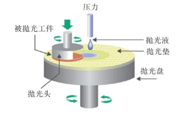
Chemical mechanical polishing (CMP) is a key process in chip manufacturing used to achieve wafer surface planarization. During polishing, the workpiece surface first undergoes a chemical reaction with substances in the polishing slurry, generating a relatively easy-to-remove soft layer. Then, the soft layer is removed by the mechanical action of abrasive particles and polishing pads in the slurry, exposing the workpiece surface again. The chemical reaction then continues, and this alternating chemical and mechanical action completes the workpiece surface polishing, ultimately achieving the goal of surface planarization.

CMP polishing slurry is made by uniformly mixing abrasive particles, surfactants, oxidants, pH adjusters, and deionized water. The technical challenge lies in adjusting the liquid formula combination according to different polishing objects and polishing environments.
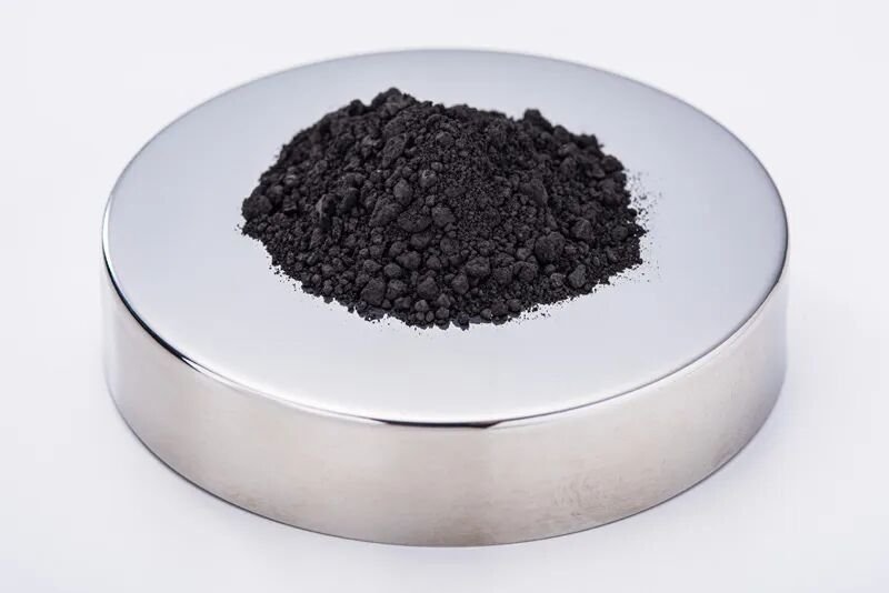
The polishing fluid abrasive is mainly composed of inorganic oxide nanoparticles, including cerium oxide (CeO2), silicon oxide (SiO2), aluminum oxide (Al2O3), manganese oxide (MnO2), zirconium oxide (ZrO2), and diamond, which can perform mechanical friction, adsorption, and removal of corrosion products.
With the miniaturization and precision of semiconductor devices, more stringent CMP polishing performance is required, such as high selectivity with high removal rates and low scratch defects, as well as self-stopping polishing slurries. CeO2 possesses a favorable crystal structure and excellent tribochemical activity, exhibiting a strong affinity for SiO2, enabling efficient removal of silicon oxide.
Furthermore, CeO2 is also a semiconductor photocatalyst, possessing variable valence states (Ce4+ and Ce3+) and abundant oxygen vacancies, combining tribochemical capabilities and photochemical oxidation activity, making it suitable for photocatalytically assisted polishing. Therefore, CeO2 has become the preferred polishing abrasive for interlayer media such as SiO2 oxides, attracting widespread attention and research.
For semiconductor (integrated circuits, chips, optoelectronic devices) manufacturing processes, the requirements for polishing precision are becoming increasingly stringent. The cerium oxide used typically needs to be at the nanoscale, but my country currently accounts for a small percentage of the global market for cerium oxide slurries that meet high-precision polishing requirements. Therefore, many researchers are dedicated to developing cerium oxide-based nanoparticles with different morphologies, sizes, and excellent surface properties to meet the polishing requirements of end-use applications.
Application of rare earth elements in magnetic components
High-end equipment such as lithography machines requires high-performance motors and magnetic bearings for precise motion control. According to experts from the Chinese Society of Rare Earths, the motion precision of these devices typically needs to reach the nanometer or even sub-nanometer level, thus placing extremely high demands on the performance of motors and bearings. Rare earth permanent magnet materials, such as neodymium iron boron (NdFeB) and samarium cobalt (SmCo), are key materials for manufacturing these high-performance components, meeting stringent requirements such as high energy product, high coercivity, high remanence, good temperature stability, and high uniformity.
Neodymium iron boron permanent magnet materials
Neodymium iron boron (NdFeB) permanent magnets possess extremely high magnetic energy product, making them among the highest-performing permanent magnet materials known to date. NdFeB materials can be used to manufacture high-performance motors that are small, lightweight, and powerful, driving precision moving parts in photolithography machines to achieve accurate alignment and scanning. With the continuous development of photolithography technology, the requirements for motion control precision are increasing, placing higher demands on the performance of NdFeB permanent magnets. Praseodymium, neodymium, terbium, and dysprosium are key rare earth elements for manufacturing high-performance NdFeB magnets.
Samarium cobalt permanent magnet materials
Samarium-cobalt permanent magnets exhibit excellent high-temperature stability, with minimal magnetic property decay at high temperatures, making them suitable for applications requiring high temperature stability. In equipment such as lithography machines, the prolonged operation generates significant heat, thus placing high demands on the temperature stability of magnetic components. Samarium-cobalt permanent magnets, containing the rare-earth element samarium, maintain stable magnetic properties even at high temperatures, ensuring the normal operation of the equipment.
Application of high-purity rare earth sputtering targets in integrated circuits
As electronic technology advances towards high performance, multifunctionality, high capacity, and miniaturization, semiconductor chips are becoming increasingly integrated and transistors are shrinking. Traditional SiO2 gate dielectric films are now prone to leakage current and even insulation failure. Currently, hafnium, zirconium, and rare-earth modified rare metal oxide films are used to address this core leakage problem. Further reducing linewidth requires the use of rare-earth gate dielectric materials with even higher dielectric constants.
With the breakthroughs and mass production of high-end integrated circuit manufacturing processes at 28nm and below in my country, the strategic demand for high-purity rare earth metal sputtering targets is urgent. As technology advances and materials evolve, the application of high-purity rare earth metal and alloy targets in the integrated circuit field will experience explosive growth.